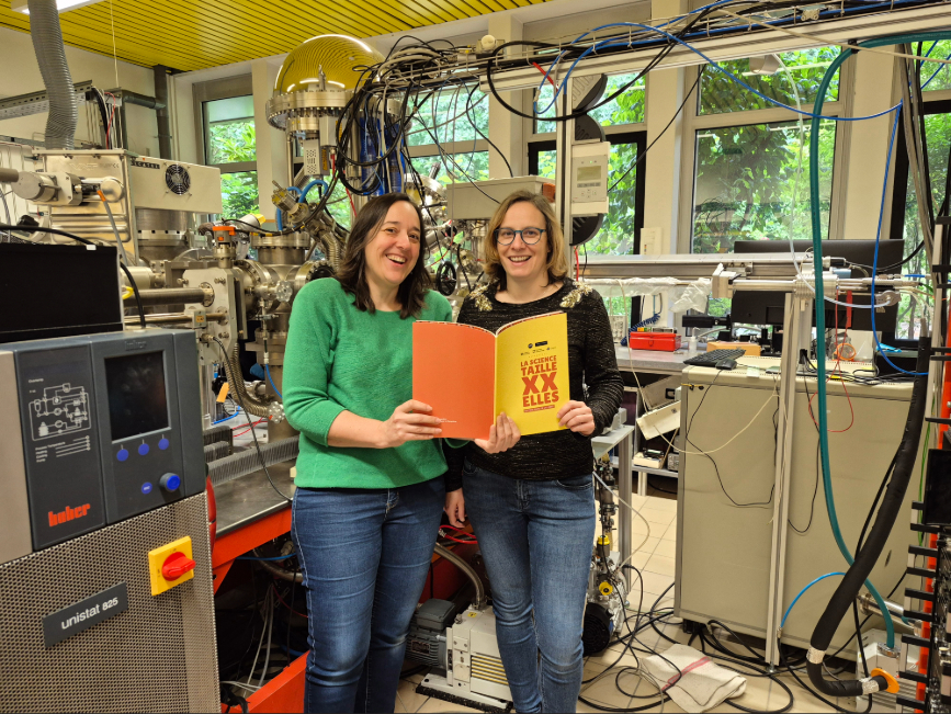
Hélène Brault and Aurélie Girard, scientific ambassadors

Our women scientists are in the spotlight! Hélène Brault and Aurélie Girard, teacher-researchers at Nantes Université and members of our laboratory, have been appointed ambassadors for the La Science taille XXelles project.
Created by the CNRS and theassociation Femmes & Sciences, the project La Science taille XXelles project aims to highlight the contributions made by women in research. Through presentations in schools, the ambassadors raise awareness among young girls of the opportunities offered by scientific and technical careers.
Hélène Brault, a chemist, and Aurélie Girard, a physicist, are carrying out complementary research dedicated to the development of new innovative materials for optics on the one hand, and electronics on the other.
Chemistry and physics are inseparable when it comes to materials innovation, and the two researchers insist on the synergy of their scientific skills. Hélène Brault develops new materials, while Aurélie Girard shapes them. Both also share a passion for teaching, passing on their knowledge to the next generation.
Within theMIOPS team, Hélène Brault is developing new crystalline materials called MOFs, for metal-organic frameworks, based on lanthanide ions. Under irradiation, these MOFs emit light whose color varies with temperature, thus acting as veritable optical nanothermometers. In nanoparticle form, they can be used in complex environments such as the human body, where they can be excited by infrared light to measure temperature at a distance, including at the level of specific organs. “These materials pave the way for key applications, such as miniature thermal cameras or early cancer detection, as cancer cells are two to five degrees warmer than healthy cells.”
Alongside her colleagues in thePCM team, Aurélie Girard studies and optimizes the way plasmas (ionized gases) interact with materials on the nanometric scale, in order to improve micro- and nano-manufacturing processes used, for example, in microelectronics and sensors. It treats and etches the surface of materials on an atomic scale, using plasmas and very low (cryogenic) temperatures. The aim is to create patterns or structures, again on a nanometric scale, to give components precise functionality.
Share this article
Other articles